Introduction:
In the intricate world of electronics manufacturing, Printed Circuit Board (PCB) assembly is a crucial stage that can make or break the functionality and reliability of electronic devices. In this blog post, we explore the top five mistakes to avoid during the PCB assembly process, and the intricacies contributing to a perfect final product.
Inadequate Component Placement:
One of the critical processes of PCB assembly service is Component placement. Accurate positioning is not just about adhering to design guidelines; it’s about orchestrating a layout that considers signal integrity, thermal dynamics, and the overall aesthetic of the PCB.
Failure in precise component placement can lead to issues, from signal integrity problems to thermal concerns. To mitigate this risk, leveraging automated assembly equipment becomes instrumental, minimizing the potential for human error and enhancing precision.
Strategically grouping high-power components can prevent localized overheating, ensuring the overall reliability of the PCB. A thorough review of the design, coupled with consultations with thermal simulation tools, becomes the sheet music guiding the placement of each component for optimal heat dissipation.
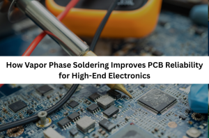
Inadequate Soldering Techniques:
The art of soldering, often overlooked as routine, holds the power to shape the destiny of a PCB.
Investing in high-quality soldering equipment and employing skilled technicians is non-negotiable. However, the journey towards soldering mastery extends beyond the basics. Employ automated soldering techniques like reflow soldering, introducing consistency, and reducing the likelihood of defects.
Regular inspections through visual examination or automated optical inspection (AOI) are the careful conductor, catching soldering issues early in the assembly process. Each solder joint is a note in the symphony, and its quality is paramount to the harmony of the final composition.
Inadequate Stencil Design and Printing:
Inadequate stencil design or printing is akin to a shaky hand, resulting in uneven solder paste application and compromising overall performance.
The art of stencil design goes beyond functionality. It ensures that the design aligns seamlessly with the PCB layout, with apertures of the correct size and shape for each component. Regular inspections and cleaning of the stencil prevent the accumulation of solder paste in undesired areas, preserving the integrity of the design.
Introducing quality control measures, such as Solder Paste Inspection (SPI), transforms stencil-related issues from potential pitfalls to opportunities for refinement. Each stencil stroke contributes to the final assembly’s artistic precision.
Neglecting ESD (Electrostatic Discharge) Precautions:
Creating a controlled environment with low humidity levels becomes the conductor’s baton, mitigating the risk of static discharge. ESD-safe packaging for components and regular ESD audits are the notes that ensure a static-free assembly environment, preserving the harmony of the entire assembly process.
Insufficient Testing and Quality Control:
The final act unfolds in the form of testing and quality control. Failing to implement robust measures in this phase is a mistake. Post-assembly testing, including in-circuit (ICT) and functional testing, identifies and rectifies defects introduced during the assembly process.
A comprehensive quality control plan ensures the final product meets and exceeds the required standards and specifications.
The PCB Layout and Assembly Process:
The PCB layout is the blueprint, and a well-designed layout contributes to the efficiency and reliability of the final product.
Simultaneously, the PCB assembly process involves the meticulous execution of each step, from component placement and soldering to testing and quality control. The PCB layout and assembly process are intertwined, influencing the other to create a functional and reliable PCB.
Conclusion:
In Printed Circuit Board assembly, avoiding mistakes is not just a process; it’s an art form. Roots EMS is one of the best PCB Assembly companies in India providing the country’s perfect EMS solutions. Attention to component placement, mastering soldering techniques treating stencil design, sparking creativity in ESD precautions, and Testing and quality control measures are the notes that create a masterpiece.
When approached with creativity and precision, the PCB assembly process transforms from a routine task into a symphony of innovation, ensuring functionality and a harmonious blend of technology and artistry.